How to Bring Back Another Amp in Ic Eagle
First Project in Eagle — 555's Flasher
Using 555 IC & Discrete Components—Eagle Series—Episode #03
![]()
In this post, we will come to grips with EAGLE and create the schematic and board files for a simple project that uses a 555 timer to flash a light-emitting diode (LED:)
In this first experiment, we will use Fritzing artifacts to convey all concepts and then use Eagle on its own.
Let's get started!
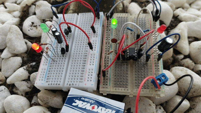
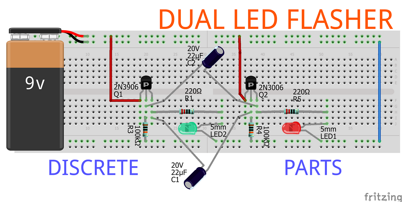
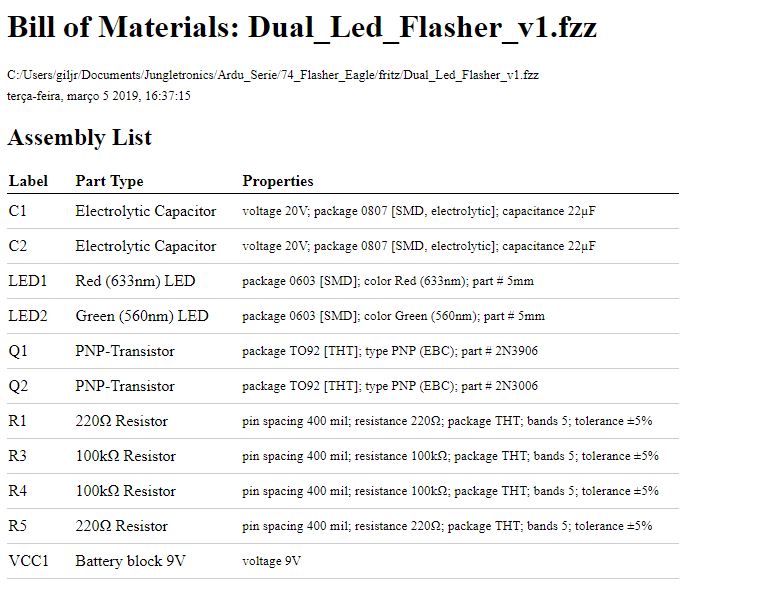
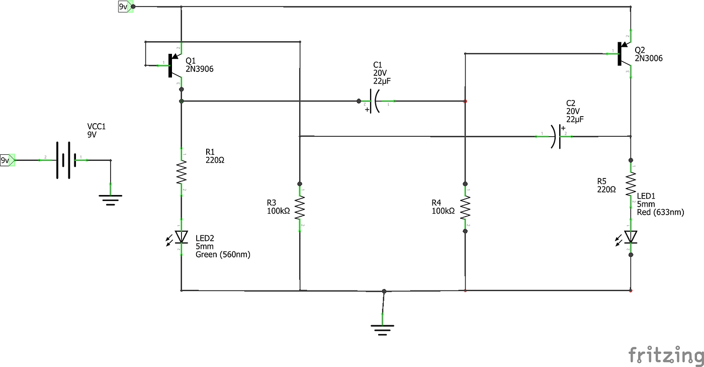
Dual LED Flasher Using Discrete Components:
Now
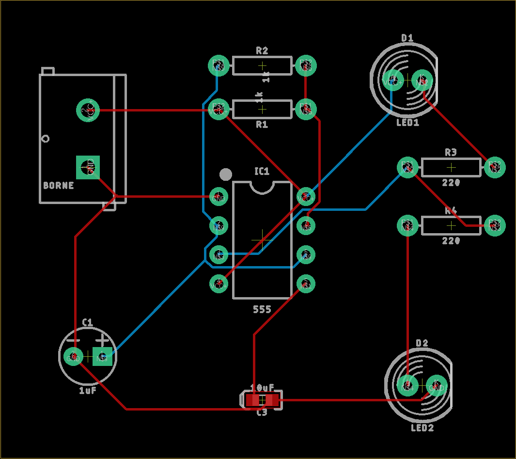
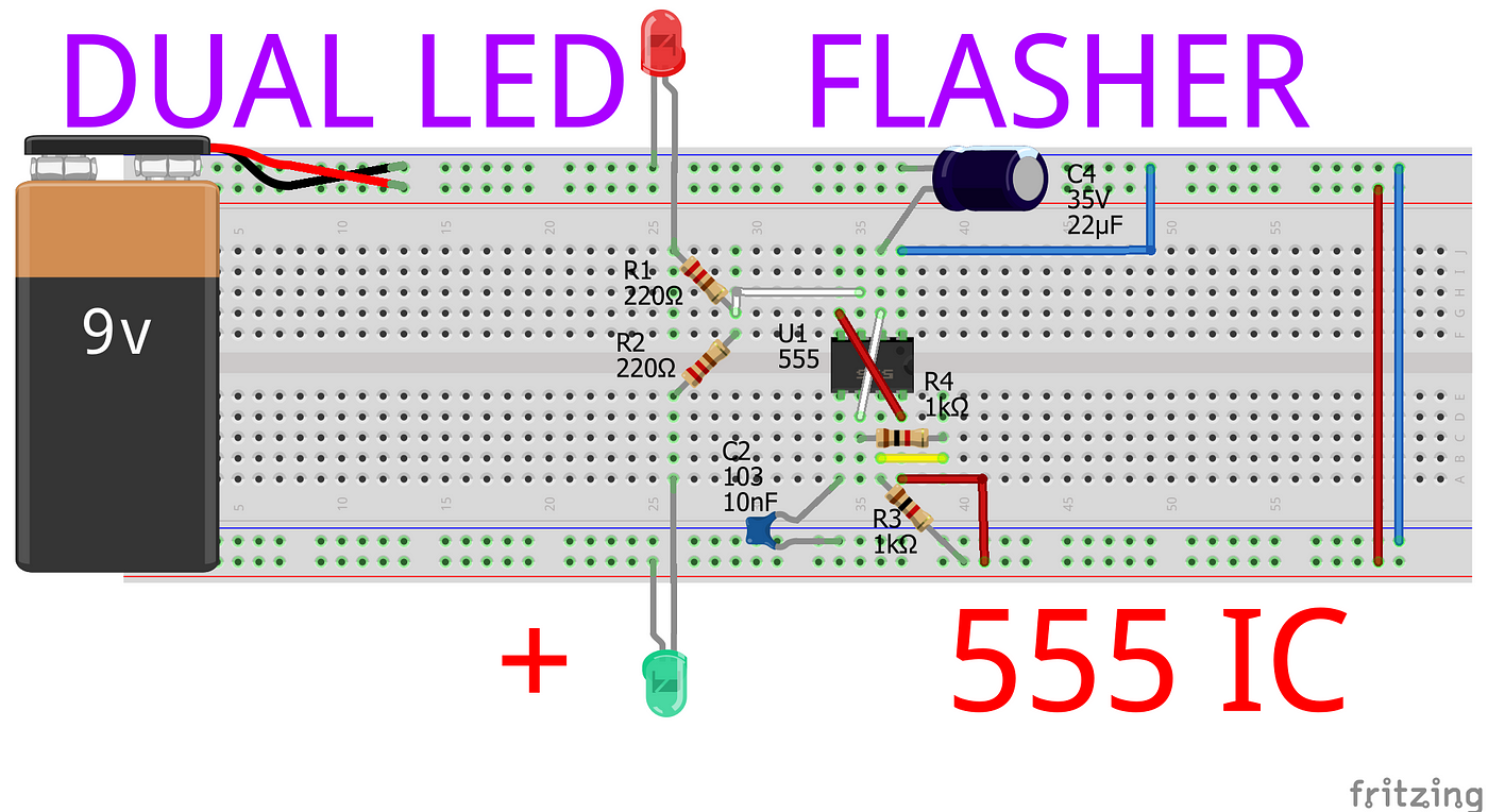
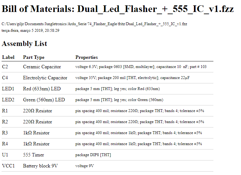
Dual LED Flasher + 555 IC:
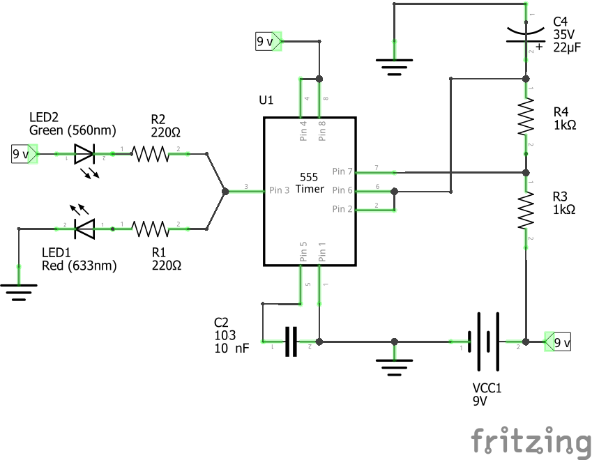
Every Problem Has At Least Two Solutions:)RIGHT?
Now, let's see that last project, DLF_555_v1, in Eagle solution:
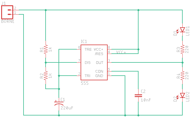
If you compare with the previous fritzing schematic now this one is a much clear one, right?
Sure, if we change our perspective with Eagle, our job is more likely to get paid. It's more professional finished, isn't it?
The Board:
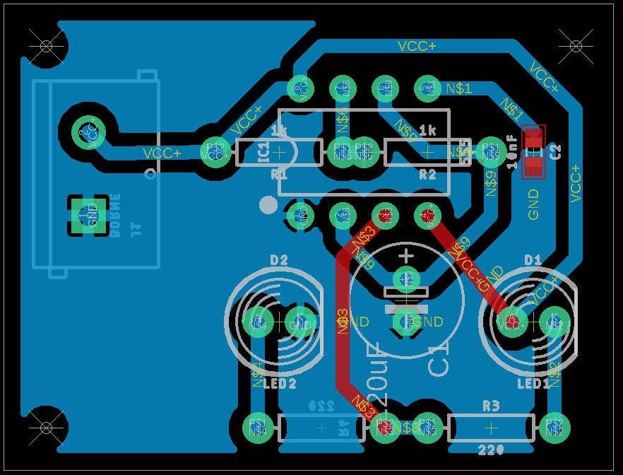
In this version, we tweak a bit of our initial design (see in these videos below) I make a step-by-step to that wonderful board). We use a ground plane.
A ground plane, as the name suggests, adds a large area of copper on the board that is connected to ground. Because quite a lot of the components have a connection to ground, this actually reduces the number of tracks required on the bottom layer, making it more likely reduces the number of tracks.
In these videos below I will explain all you need to know to get this board done :)
That's all for now!
In the next episode, we're gonna see advanced PCB feature like CAM, generating Garber files and much more…
Stay tuned!
Bye!
Download All Files For The Project:) EGL_00 EGL_01
Notes from SparkFun Ondo88: I know the tutorial it's kind of old by now, but anyway, I've some extra tips that might help someone. Tenting: It's not only about having a better silkscreen on the board, soldermask will also protect your precious vias from rust and aging. It's almost mandatory on RF and analog precision circuits. Without them CuO (copper oxide) will form a thin layer over your vias and pads, ruining your impedance adaptations. Pads are protected in part by solder additives, but it's not a bad idea to use proper spray isolators on harsh enviroments. Some PCB software offer "tear" connections for pads and vias. http://dangerousprototypes.com/forum/download/file.php?id=6979&t=1 That is an example of what I'm talking. This reduces mechanical stress around the via connection, avoiding possible rupture of the traces. Again, it's also useful for RF applications, as it makes a better Z matching (it behaves as a tamper used in micro-wave circuits). In PCB software without this kind of feature, you can made your own tear connections manually if you're concerned about some of that issues. It's a good practice to place holes around the boards, joining top and bottom ground layers. That makes the board more similar to a Faraday cage, reducing greatly effects from EMI (Electro-magnetic Interference). I had a board with that kind of problems, nothing worked ok until I placed the holes, it worked like a charm since then. If you like to make beautiful boards as I do, you'll probably place that holes equidistant on the perimeter, but to be truth, randomizing the distance between the holes makes a better isolation as no single frequency gets benefited form constructive interference. Get to know what you're building. Before getting serious about PCB design, you should learn what is everything you're using on them. I've always said you can know if someone is a good PCB designer by asking him to give you FR4 permitivity, solder fusion temperature and the like (without checking wikipedia ;D). When you make electronic design sometimes you can forget about physics, so be sure you know them well. Another common mistake is not taking account of thermal activity on the board. Make sure your temperature sensitive components (like oscillators, and almost any analog circuit) are far from your heat generating circuits (regulators and the like). If your board fits in a box, be sure to have cooling paths that keep the things ok. Remember that heat goes up! (so don't put your sensitive devices on the top if you can avoid that). Some chips may have two Vcc or GND pins one to each other. On SMD packages it's tempting to just join them straight, avoid that if you're using oven soldering (very likely on production). That will unbalance the thermal forces your chip may suffer, moving it from its original position, and possibly making it tombstone. I've found very useful to place a couple of squares on silkscreen, with an E (Error) and a T (Tested) on the side of each one. That allows you to mark easily your boards with anything you may have at hand, from a pen to a screwdriver. The last one is the more ethereal of the advises, "follow your ground paths". Your signal propagates from your Vcc to your GND, mainly through the shortest path, if two signals share that ground path, they'll interfere each other. Try to make that paths as short and trouble free as you can. and most important, Have fun with your PCBs :D
Related Posts (in construction…)
EAGLE Series — Homemade PCB — Series Intro & Motivations — Episode #01
Installing Eagle & Terminology — Concepts & Installations — Episode #02
First Project in Eagle — 555's Flasher — Eagle Series — Using 555 IC & Discrete Components — Episode #03
Eagle Project — Simple PCB Etchant — The Whole Process — Episode #04
Credits & References
Computer-Aided Manufacturing (CAM)
Schematic Basics Part 3: Checking Connectivity Errors with an ERC in Autodesk EAGLE
SparkFun/SparkFun-Eagle-Libraries
adafruit/Adafruit-Eagle-Library
Seeed-Studio/OPL_Eagle_Library
simonmonk/eagle
The EAGLE Schematic & PCB Layout Editor — A Guide
Better PCBs in Eagle
SparkFun Electronics Eagle Rules
TOP 10 PRINTED CIRCUIT BOARD DESIGN CHECKS Download Now: pdf
How to Install and Setup EAGLE
Eagle PCB Tutorial: Custom Library
Custom PCBs Made Simple by JLC
EAGLE Library Structure
E agle Series Videos:
#01 https://youtu.be/e1ERSU91-PY
#02 https://youtu.be/SLnq33xqd54
#03 https://youtu.be/g8AdpwRkVj0
#04 https://youtu.be/R25o4irzqTY
#05 https://youtu.be/gRsiuOdpVMA
Solar Turret V2 Project: https://youtu.be/TDLHVimV0FM
Tutorial Eagle (em Português) do canal fabuloso youtube MrAppleBR (VLW Nilton, tamos juntos:)
— First Published at Mar@2019 —
How to Bring Back Another Amp in Ic Eagle
Source: https://medium.com/jungletronics/first-project-in-eagle-555s-flasher-d4d1fa822537
0 Response to "How to Bring Back Another Amp in Ic Eagle"
Post a Comment